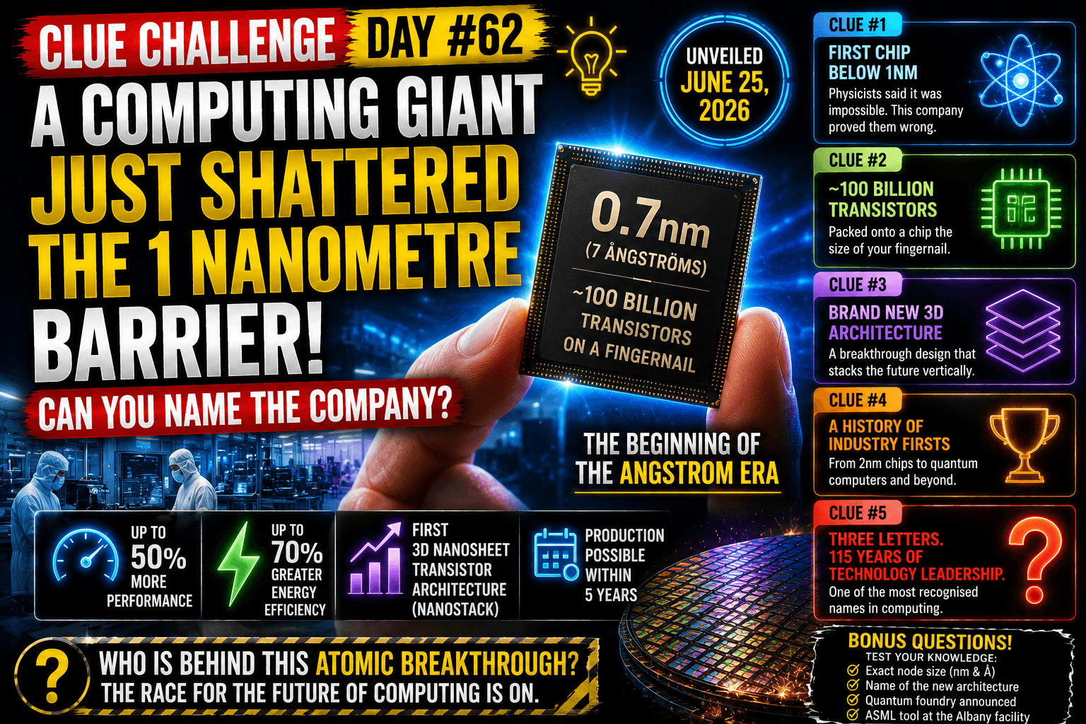
One company. Five clues. 100 billion transistors on a fingernail. Unveiled June 25, 2026. The most important chip breakthrough in a decade. All real.
For decades, physicists said it was impossible — that transistors could not shrink below one nanometer without hitting the physical limits of atomic matter itself. This week, a 115-year-old American technology company proved them wrong. Can you name the company before the final clue?
Clue #1 — It just packed 100 billion transistors onto a chip the size of your fingernail
On June 25, 2026, a major American technology company unveiled the world’s first sub-1 nanometre chip — operating at 0.7 nanometres, or 7 angstroms — a unit so small it approaches the scale of individual atoms.
The new chip packs nearly 100 billion transistors onto a surface the size of a fingernail — nearly twice the density of its own previous-generation chip unveiled in 2021.
Early technical results project the chip delivers up to 50% more performance — or 70% greater energy efficiency — compared to that previous generation. The implications span generative AI, cloud infrastructure, and next-generation consumer devices.
“This industry-first innovation sets the foundation for the next era of computing,” said the Director of Research at the company — an [Company Name] Fellow named Jay Gambetta.
Clue #2 — It invented a brand-new transistor architecture — in three dimensions — called “nanostack”
Every chip generation before this one stacked transistors flat — in two dimensions — shrinking them progressively smaller according to a pattern that has governed the semiconductor industry since 1965.
This company broke that pattern entirely.
Its researchers developed a three-dimensional transistor architecture called nanostack — the industry’s first known 3D nanosheet-based design — which vertically stacks and staggers transistors, using different material combinations in each layer to optimise performance and power efficiency independently.
The nanostack architecture was experimentally validated through ultra-thin dielectric bonding in CMOS integration, demonstration of dual-channel engineering capability, and functional CMOS inverter operation. Results presented at VLSI 2026 confirmed it delivers 40% scaling in SRAM — unlocking dramatically more efficient chip designs capable of handling advanced AI workloads.
Clue #3 — It previously invented the 2nm chip, nanosheet transistors, and the first quantum computer available on the cloud
This company does not just build chips. It has led the entire semiconductor industry through every generational transition since the 1960s.
It invented the nanosheet transistor architecture — now the entire industry’s leading-edge standard — before moving beyond it with nanostack. It unveiled the world’s first 2nm chip in 2021. It built the first quantum computer made available on the cloud. And just this month, alongside this chip announcement, it revealed plans to spin off a standalone quantum foundry — called Anderon — to manufacture quantum wafers for the United States and its partners.
A company that invented the nanosheet. Then invented what comes after it.
Clue #4 — It is racing against TSMC, Intel, and Huawei’s Tau Scaling Law — and just took the lead
The semiconductor industry in 2026 is the most competitive in history. Taiwan’s TSMC — the world’s largest chip manufacturer — currently uses 2nm technology and plans to introduce 1.4nm by 2028. Intel is targeting similar timescales. And Huawei, as readers of Clue Challenge Day #31 will remember, unveiled the Tau Scaling Law in Shanghai in May 2026 — declaring that Moore’s Law is dead and proposing a new principle based on time scaling rather than transistor shrinkage.
This company’s response: 0.7nm. Validated in a laboratory. Working devices confirmed. Production possible within five years.
One angstrom-era chip. The entire global semiconductor order suddenly reshuffled.
Clue #5 — It was founded 115 years ago — its three-letter name is one of the most recognised in the history of computing
This is your final clue — and your most direct.
The company behind the world’s first sub-1nm chip was founded in 1911. It is headquartered in Armonk, New York. Its semiconductor research is conducted at a facility in Albany, New York — soon to house a High-NA EUV lithography tool developed by ASML. Its partners on this project include Lam Research, Tokyo Electron, and SCREEN Semiconductor Solutions.
Its three-letter name has been synonymous with computing since the mainframe era. Its initials stand for a phrase that describes the nature of its business — and has done so for over a century.
Three letters. Blue logo. The company that once built the machines that put humans on the Moon — and just built the transistor that may power the machines that take humans to Mars.
So — which company is it?
Founded 1911. Headquartered Armonk, New York. Unveiled the world’s first sub-1nm chip on June 25, 2026. Architecture: nanostack — the world’s first 3D nanosheet-based transistor design. Density: 100 billion transistors per fingernail. Performance gain: up to 50%. Energy efficiency gain: up to 70%. Production timeline: within five years. Also announcing a standalone quantum foundry called Anderon this same week. Three-letter name. Blue logo. One of the most famous abbreviations in the history of technology.
Bonus — can you name:
- The exact node size of the new chip — in both nanometres and angstroms
- The name of the new transistor architecture it invented
- The standalone quantum foundry it announced alongside this chip
- The ASML tool being installed at its Albany research facility
Drop your answer below. Unlike Wordle, this one is measured in atoms. Day #63 arrives tomorrow.
Missed yesterday’s challenge?
Answer to Yesterday’s Challenge: DAY #61
(Click above to reveal)