
The global semiconductor race has entered a new phase. For decades, chipmakers competed by making transistors smaller under Moore’s Law. But as physical limits, soaring costs, and geopolitical restrictions make further miniaturization increasingly difficult, Huawei has proposed a radically different path.
At the IEEE International Symposium on Circuits and Systems (ISCAS) 2026 in Shanghai, Huawei unveiled two major concepts—Tau (τ) Scaling Law and LogicFolding. Together, they aim to deliver 1.4nm-class chip performance by 2031 without relying on ASML’s Extreme Ultraviolet (EUV) lithography machines, access to which has been restricted by U.S. export controls.
Why Is Huawei Looking Beyond Moore’s Law?
For nearly 60 years, Moore’s Law guided semiconductor progress by doubling transistor density approximately every two years. Smaller transistors meant faster, more efficient chips.
However, this model faces growing challenges:
- Rising manufacturing costs
- Physical limits of silicon
- Increasing power consumption
- Dependence on expensive EUV lithography
- Geopolitical restrictions on advanced chip equipment
Huawei argues that future performance gains should come not only from shrinking transistors but also from redesigning how chips are built and how quickly information moves inside them.
What Is the Tau (τ) Scaling Law?
The Greek letter τ (Tau) represents signal propagation delay—the time electrical signals take to travel through a chip.
Huawei’s Tau Scaling Law focuses on reducing this delay rather than simply shrinking transistor size.
Instead of asking “How can we make transistors smaller?”, Tau Scaling asks:
“How can we make information travel faster?”
By shortening signal paths, reducing latency, and improving communication between chip components, Huawei believes older manufacturing processes can achieve performance comparable to much smaller process nodes.
Some analysts describe Tau Scaling as an evolution beyond Moore’s Law—from transistor scaling to communication scaling.
What Is LogicFolding?
LogicFolding is the physical architecture implementing Tau Scaling.
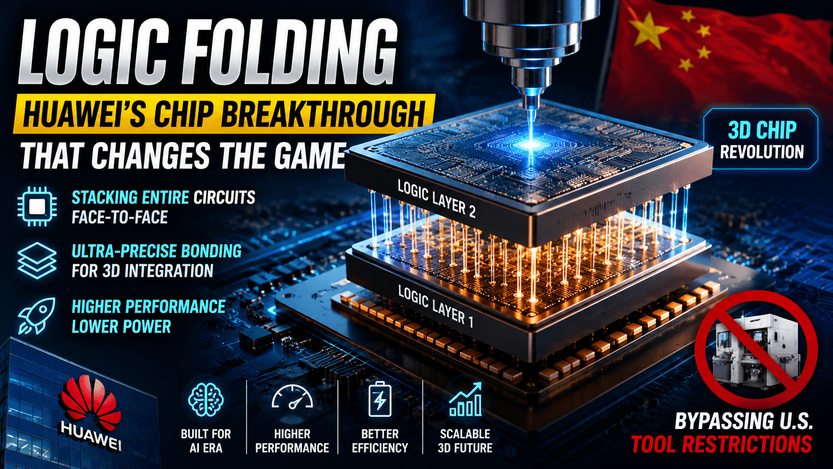
Instead of placing all logic circuits on a single flat silicon layer, Huawei stacks complete logic circuits face-to-face using ultra-precise hybrid bonding.
This creates a compact three-dimensional chip where data travels much shorter distances.
Imagine replacing a sprawling one-story factory with a high-rise building where departments are stacked vertically. Workers—and in this case, electrical signals—spend far less time moving between floors than crossing a vast horizontal campus.
How LogicFolding Works
The technology involves three key innovations:
- Face-to-face stacking: Two logic layers are bonded together with microscopic precision.
- Hybrid bonding: Dense vertical interconnects replace longer horizontal wiring.
- UnifiedBus interconnect: A new system-level communication fabric designed to reduce latency between chips in Huawei’s AI computing clusters.
According to Huawei, this architecture delivers:
- 55% higher transistor density
- 41% better power efficiency
- Faster communication between chip components
- Lower energy consumption
- Higher computing performance for AI workloads
The company plans to introduce the technology in its next-generation Kirin processor powering the Mate 90 smartphone series before extending it to Ascend AI accelerators and large-scale AI data centres.
Can Huawei Really Build 1.4nm Chips Without EUV?
This is where an important distinction must be made.
Huawei is not claiming to manufacture true 1.4nm transistors comparable to those expected from TSMC’s A14 process.
Instead, the company aims for 1.4nm-equivalent transistor density by stacking multiple logic layers rather than shrinking individual transistors.
In other words:
- TSMC: Achieves higher density by making transistors physically smaller.
- Huawei: Achieves similar density by arranging chips vertically.
This represents a shift from node scaling to system-level integration.
Why It Matters
Huawei’s announcement comes amid the ongoing U.S.-China semiconductor rivalry. Since 2019, U.S. export controls have restricted China’s access to advanced chips, NVIDIA AI accelerators, and ASML’s EUV lithography systems.
LogicFolding demonstrates China’s broader strategy of achieving technological self-reliance through alternative engineering approaches rather than waiting for access to restricted technologies.
If successful, it could reduce China’s dependence on foreign manufacturing tools while strengthening domestic AI and semiconductor capabilities.
Challenges Ahead
Despite its promise, several hurdles remain:
- Mass production at commercial scale
- Managing heat in stacked chips
- Manufacturing yield and reliability
- Independent verification of Huawei’s performance claims
- Competition from advanced packaging technologies developed by TSMC (SoIC, CoWoS), Intel (Foveros), Samsung (X-Cube), AMD (3D V-Cache), and NVIDIA
The Bigger Picture
The semiconductor industry is entering a post-Moore era where advanced packaging, chiplet architectures, 3D stacking, and system integration may become as important as transistor miniaturization. Huawei’s Tau Scaling Law and LogicFolding signal this transition, showing that the future of chip design may depend not just on smaller transistors, but on smarter architectures.
Key Takeaway
Huawei’s LogicFolding and Tau Scaling Law represent one of the boldest attempts to rethink semiconductor design. By focusing on reducing signal delay instead of simply shrinking transistors, the company hopes to achieve 1.4nm-class performance by 2031 without relying on ASML’s EUV machines. Whether these claims translate into large-scale commercial success remains to be seen, but the announcement has already intensified the global debate over the future of semiconductor innovation in an era shaped by both technological limits and geopolitical competition.
Reference: Huwaei