
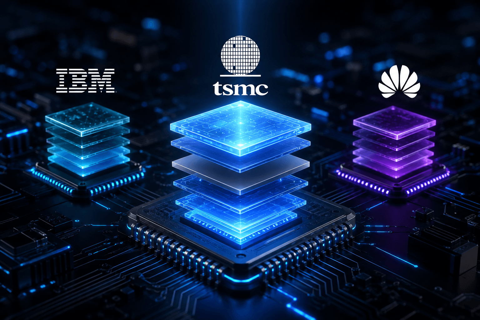
The semiconductor industry entered the Angstrom era while simultaneously redefining Moore’s Law through 3D stacking, advanced packaging, chiplets, backside power delivery, silicon photonics, and AI-first architectures. Instead of relying solely on transistor shrinking, manufacturers are engineering performance across the entire chip stack.
Major Lithography & Process Leaps
IBM Nanostack (0.7nm / 7Å) (Research Prototype)
- World’s first publicly demonstrated sub-1nm CMOS technology
- Around 100 billion transistors on a fingernail-sized chip
- Introduces 3D staggered transistor stacking
- Around 2× logic density
- ~40% SRAM scaling
Why it matters: Demonstrates how vertical integration could extend Moore’s Law beyond traditional planar scaling.
TSMC A16 (1.6nm)
- Angstrom-generation process
- Super Power Rail (Backside Power Delivery Network)
- 8–10% higher performance
- 15–20% lower power than N2P
- Mass production targeted for late 2026
Breakthrough
- Backside power
- NanoFlex Pro optimization
- Better AI efficiency
Intel 18A (1.8nm-class)
- RibbonFET (Gate-All-Around)
- PowerVia backside power delivery
- First commercial use of High-NA EUV on selected production layers
- Panther Lake launches the technology commercially
Why it matters
Intel becomes the industry’s first company to ship commercial High-NA EUV-produced logic chips.
TSMC N2 (2nm)
- First mass-produced TSMC GAA process
- Nanosheet transistors
- Better leakage control
- Significant efficiency improvements for AI and mobile chips
Key New Chip Architectures
IBM Nanostack
- Vertical transistor stacking
- 2× density
- SRAM innovation
- Beyond FinFET and GAA
AMD Instinct MI455X (MI400 Family)
- Advanced chiplet architecture
- HBM4 memory
- Designed for Helios AI infrastructure
- Massive AI inference throughput
NVIDIA Rubin / Vera Rubin
- Dual-reticle architecture
- NV-HBI interconnect
- HBM4 memory
- Blackwell successor
Rubin pushes AI scaling through packaging rather than simply increasing monolithic die size.
Google TPU 8t / TPU 8i
Google separated its AI hardware into dedicated:
- Training processors
- Inference processors
This specialization improves efficiency for hyperscale AI workloads.
Huawei Kirin 2026 – LogicFolding (Company Research/Prototype Direction)
Huawei introduced:
- Tau (τ) Scaling Law
- LogicFolding
- Vertical logic stacking
- Hybrid bonding
Instead of relying only on smaller transistors, Huawei proposes optimizing time-domain efficiency (τ) across architecture, software, packaging, and manufacturing. Company research reports significant power savings and projects density improvements over future generations, though long-term targets remain forward-looking.
Memory Breakthroughs
HBM4 Enters Commercial AI
2026 marks the transition from HBM3E toward HBM4.
Benefits include:
- Higher bandwidth
- Larger memory capacity
- Lower latency
- Essential for trillion-parameter AI models
Memory bandwidth—not compute—has become the primary bottleneck for many AI workloads.
Silicon Photonics
One of the biggest trends of 2026 is replacing electrical interconnects with optical links.
Advantages include:
- Higher bandwidth
- Lower latency
- Lower energy per bit
- Better AI cluster scalability
Major companies—including NVIDIA, Intel, TSMC, Broadcom, and hyperscalers—are investing heavily in co-packaged optics.
AI-Specific Architecture Trends
Instead of designing general-purpose processors, chipmakers increasingly optimize for AI workloads through:
- Chiplets
- Domain-specific accelerators
- Memory-centric compute
- Sparse computation
- Low-precision formats (FP4/FP6/FP8)
- On-package networking
This represents one of the biggest architectural shifts since the GPU.
2026 Defining Trends
Lithography
- High-NA EUV enters production
- Angstrom-era nodes (1.6–2nm)
- Sub-1nm research accelerates
Architecture
- Gate-All-Around
- RibbonFET
- 3D stacking
- Chiplets
- Backside power delivery
- Hybrid bonding
Packaging
- CoWoS
- SoIC
- Foveros
- UCIe
- HBM4 integration
AI
- Dedicated training and inference chips
- Memory-first architectures
- Silicon photonics
- Optical interconnects
New Paradigms
- IBM Nanostack explores vertical transistor scaling.
- Huawei’s Tau Law and LogicFolding propose optimizing compute beyond geometric transistor shrinkage.
- Advanced packaging is emerging as the industry’s “new Moore’s Law.”
Final Take
The semiconductor industry in 2026 is no longer defined solely by smaller transistors. Leadership now depends on combining Angstrom-class lithography, 3D integration, advanced packaging, high-bandwidth memory, silicon photonics, and AI-native chip architectures. IBM’s Nanostack demonstrates the future of vertical transistor scaling, Intel and TSMC are commercializing the Angstrom era, while AMD, NVIDIA, Google, and Huawei are rethinking how AI processors are built. The next decade of chip innovation will be driven as much by how chips are connected and stacked as by how small their transistors become.
Additional noteworthy 2026 developments to mention
- SK hynix HBM4 sampling and ecosystem ramp-up for next-generation AI accelerators.
- Micron HBM4 roadmap progress targeting AI infrastructure.
- Broadcom Tomahawk 6 Ethernet switch, delivering 102.4 Tbps for AI fabrics—highlighting that networking chips are becoming as critical as compute chips.
- Growing adoption of co-packaged optics (CPO), a major step toward optical AI data-center interconnects.