
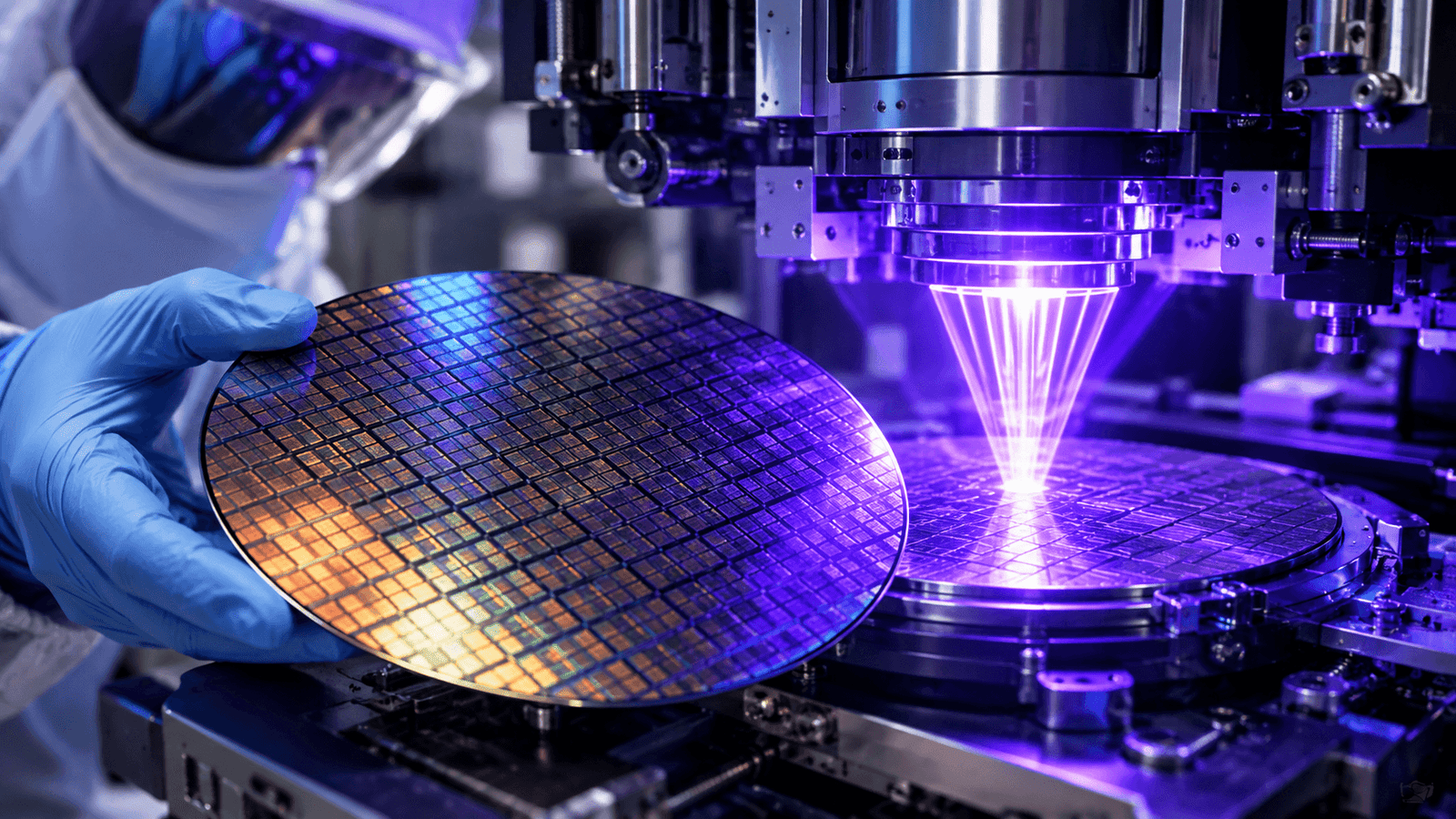
In the race to manufacture the world’s most advanced semiconductors, two photolithography technologies dominate discussions: Deep Ultraviolet (DUV) and Extreme Ultraviolet (EUV). As of August 2026, the contrast between these approaches has sharpened due to major breakthroughs on both sides. Understanding DUV vs EUV is essential for anyone following chipmaking, AI hardware demand, or geopolitical technology competition.
What Is DUV vs EUV Lithography?
DUV lithography uses light at approximately 193 nm wavelength generated by ArF excimer lasers. Modern systems rely on immersion techniques (water between the lens and wafer) to improve resolution. It remains highly mature, cost-effective, and widely used for non-critical layers and mature process nodes.
EUV lithography operates at a much shorter 13.5 nm wavelength. This enables finer circuit patterns with fewer process steps. Standard Low-NA (0.33) EUV tools have been in high-volume manufacturing for years. The next generation, High-NA EUV (0.55 numerical aperture), delivers even better resolution—targeting roughly 8 nm half-pitch in a single exposure.
The fundamental advantage of EUV is resolution. The practical advantages of DUV are lower cost, higher mature throughput, and established infrastructure.
Latest 2026 Lithography Developments
Two major stories defined the DUV vs EUV landscape in mid-2026.
First, China achieved a significant milestone in domestic immersion DUV production. In late July 2026, a state-backed Shanghai company (Shanghai Aishengna Electronic Technology Group, incorporating teams from firms including Yuliangsheng) began mass-producing immersion DUV lithography machines. Plans call for approximately five systems in 2026 and around 20 in 2027. Initial customers include SMIC, Hua Hong Semiconductor, and ChangXin Memory Technologies (CXMT). These tools primarily target 28 nm single-exposure processes and can support multi-patterning toward 7 nm-class chips. While performance lags the latest ASML systems (roughly comparable to older designs), the development marks real progress in China’s self-reliance efforts under export controls. Volumes remain small compared with ASML’s planned ~130 immersion DUV shipments in 2026.
China’s EUV program remains further behind. A prototype was reported operational in late 2025, but light source power (100–150 W), mirror reflectivity, and photoresist quality still trail commercial requirements. Full production capability is still years away.
Second, High-NA EUV reached a commercial production milestone. On July 15, 2026, ASML confirmed that Intel Foundry became the first company to use High-NA EUV tools in high-volume manufacturing. Specific layers of Intel Core Ultra Series 3 processors (Panther Lake) on the 18A process are being patterned with these systems, achieving yields matching standard Low-NA platforms. Intel has led adoption, while Samsung is installing tools and TSMC continues to prioritize cost-efficient extension of existing Low-NA EUV technology for the near term.
ASML simultaneously raised its 2026 revenue guidance to €43–45 billion, citing strong AI-driven demand, and announced plans to expand both EUV and DUV production capacity by roughly 30% annually in 2027 and 2028.
DUV vs EUV Lithography Comparison
| Factor | DUV (Immersion) | EUV (Low-NA + High-NA) |
|---|---|---|
| Wavelength | ~193 nm | 13.5 nm |
| Primary Strength | Cost, maturity, throughput for many layers | Superior resolution, fewer process steps |
| Current Role (2026) | Majority of layers; mature nodes; multi-patterning for advanced chips without EUV access | Critical layers on leading-edge nodes (3 nm, 2 nm, 18A and below) |
| Latest Progress | China begins limited domestic production | High-NA enters commercial HVM at Intel |
| Cost & Complexity | Lower tool and operating costs | Significantly higher (High-NA tools especially expensive) |
| Geopolitical Factor | More accessible; China advancing domestically | Strict export controls; ASML monopoly |
Outlook for Chipmakers and the Industry
Leading foundries continue a hybrid strategy. TSMC, Samsung, and Intel use EUV extensively for the finest features while relying on DUV for the bulk of patterning steps. AI demand is accelerating orders for both technologies, with ASML expanding capacity across the board.
For China, domestic DUV production improves supply security for mid-range and multi-patterned advanced nodes but does not eliminate the need for eventual EUV capability. The technology gap on the most advanced chips remains substantial.
In summary, DUV is not dead—it remains indispensable and is seeing capacity growth and new domestic suppliers. EUV, particularly High-NA, is the enabling technology for continued dimensional scaling and is now proven in real high-volume logic production. The DUV vs EUV debate in 2026 is less about replacement and more about complementary roles in an industry racing to meet unprecedented demand for advanced silicon.
As process nodes shrink further and geopolitical pressures persist, both technologies will shape the semiconductor landscape for years to come.