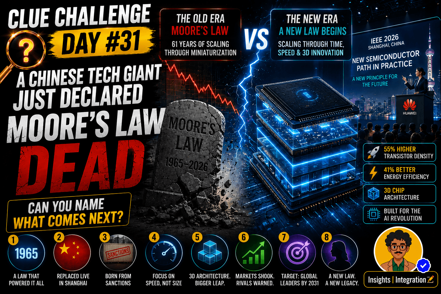
A daily puzzle for curious minds. One breakthrough. Eight clues pulled from this week’s biggest technology headlines. All real. All happening now.
For more than 60 years, one idea quietly powered the modern world.
Every iPhone.
Every AI model.
Every gaming console.
Every cloud server.
Every supercomputer.
But this week, at one of the world’s largest semiconductor conferences, a Chinese tech giant stood on stage and declared that era over.
In its place: a brand-new law for the future of computing.
The announcement immediately shook the semiconductor industry, triggered debate across Silicon Valley, and reignited the global US–China tech race.
Can you identify it before the final clue?
The Clue Challenge
Clue #1 — One prediction built the digital age
In 1965, Intel co-founder Gordon Moore made a famous prediction:
The number of transistors on computer chips would roughly double every two years while costs stayed manageable.
That idea became known as Moore’s Law.
For decades, it drove the entire tech industry forward — making computers smaller, faster, cheaper, and more powerful.
Smartphones.
Laptops.
AI systems.
Data centers.
Everything depended on it.
But engineers have increasingly warned that shrinking transistors further is becoming physically and economically unsustainable.
And now, a new alternative has officially emerged.
Clue #2 — The announcement happened this week in Shanghai
On May 25, 2026, at the IEEE International Symposium on Circuits and Systems in Shanghai, Huawei executive He Tingbo unveiled a new semiconductor framework during a keynote titled:
“New Semiconductor Path in Practice.”
The presentation instantly became one of the most discussed moments in the global chip industry this year.
Because Huawei wasn’t simply announcing a new chip.
It was proposing an entirely new direction for computing itself.
Clue #3 — US sanctions accidentally helped create it
Back in 2019, the United States imposed major export restrictions on Huawei.
The company lost access to advanced Western chip technology and cutting-edge EUV lithography machines used for traditional transistor scaling.
Most analysts expected Huawei to fall behind permanently.
Instead, the company reportedly entered what executives called:
“Extreme survival mode.”
Unable to follow the traditional semiconductor roadmap, Huawei began developing alternative chip-design strategies internally over several years.
Now those experiments are being presented as a potential successor to Moore’s Law.
Clue #4 — The breakthrough focuses on speed, not transistor size
Traditional chip progress relied on making transistors physically smaller.
Huawei’s new framework takes a different approach.
Instead of focusing primarily on transistor shrinkage, it aims to reduce:
- Signal transmission delays
- Data movement time
- System communication latency
- Processing bottlenecks across entire computing systems
In simple terms:
The goal is not just smaller chips.
The goal is faster information flow across the entire architecture.
Clue #5 — It introduced a major 3D chip architecture
One of the biggest innovations tied to the framework is a system called:
LogicFolding
Instead of arranging components mostly across flat 2D layouts, the design stacks and reorganizes chip structures vertically.
Huawei claims this approach already produced:
- 55% higher transistor density
- 41% better energy efficiency
- Significant performance gains without needing the newest manufacturing nodes
The company says it has already mass-produced hundreds of chips using related methods.
Clue #6 — It became a geopolitical story immediately
The announcement landed during intensifying competition between:
- China
- The United States
- Taiwan
- Global AI chip companies
Huawei’s Ascend AI chips are now increasingly central to China’s AI ecosystem.
Meanwhile, Nvidia CEO Jensen Huang recently admitted Nvidia had “largely conceded” parts of China’s AI chip market to Huawei because of export restrictions.
The semiconductor race is no longer just about business.
It is increasingly tied to:
- National security
- AI dominance
- Supply chains
- Supercomputing
- Economic power
Clue #7 — Analysts are calling it China’s “hardware DeepSeek moment”
Many analysts compared the announcement to how Chinese AI startup DeepSeek shocked the AI industry earlier by achieving strong performance through architectural efficiency rather than sheer computing power.
The comparison matters.
Because Huawei’s new framework also attempts to bypass traditional limitations through design innovation instead of relying entirely on the world’s most advanced fabrication tools.
That could reshape how future AI infrastructure is built globally.
Clue #8 — Its creator is being called “China’s Gordon Moore”
The framework was unveiled by He Tingbo, one of Huawei’s most influential technology leaders.
Chinese researchers and tech commentators have already started referring to the concept as:
“Her’s Law”
— a play on Moore’s Law and a reference to He Tingbo herself.
During the keynote, she openly called for international scientific collaboration, saying no single company can solve the future of semiconductors alone.
Final Question
So — what is this new two-word semiconductor law?
The one that:
- Was unveiled in Shanghai in May 2026
- Claims Moore’s Law is reaching its limits
- Focuses on reducing system latency instead of only shrinking transistors
- Introduced LogicFolding 3D chip architecture
- Emerged from Huawei during US sanctions
- Could reshape the future of AI hardware and semiconductor design
Bonus Questions
Can you also name:
- The Intel co-founder behind Moore’s Law
- The Huawei 3D chip architecture tied to the breakthrough
- The AI chip series powering many of China’s newest AI systems
- The nickname researchers gave He Tingbo after the announcement
Drop your answer below before Day #32 arrives tomorrow.
Missed yesterday’s challenge?
Check it here → Clue Challenge Day #30: This Observatory Is Changing Astronomy Forever — Can You Name It?

Answer to Yesterday’s Challenge: DAY #30
(Click above to reveal)